So a variety of things are moving forward this week, though none as dramatically amazing as I might have hoped when putting together the final schedule for completing this project.
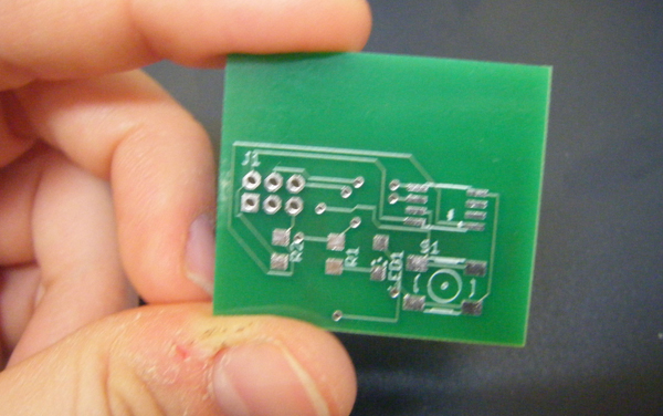
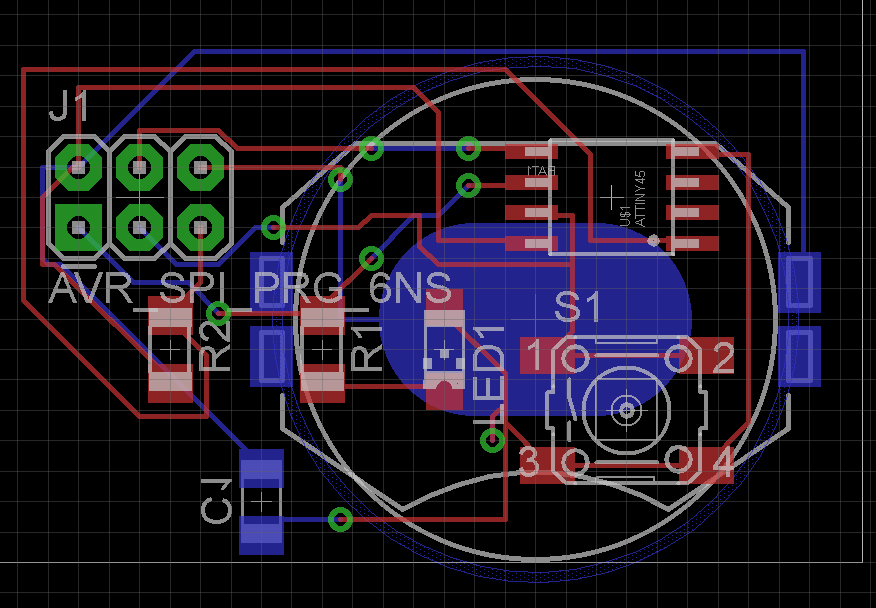
I had sent out the PCB to be printed nearly two weeks ago, and finally got it back in the mail yesterday, somewhat wrong-sized and only one! It seems they didn’t like that I put holes so that I could cut the board, or else I just did something completely wrong. In any event, I’m looking forward to stuffing and programming the board, hopefully both on Friday, and then I can see if the electronics of it will work. 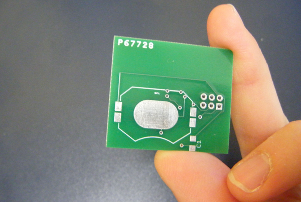
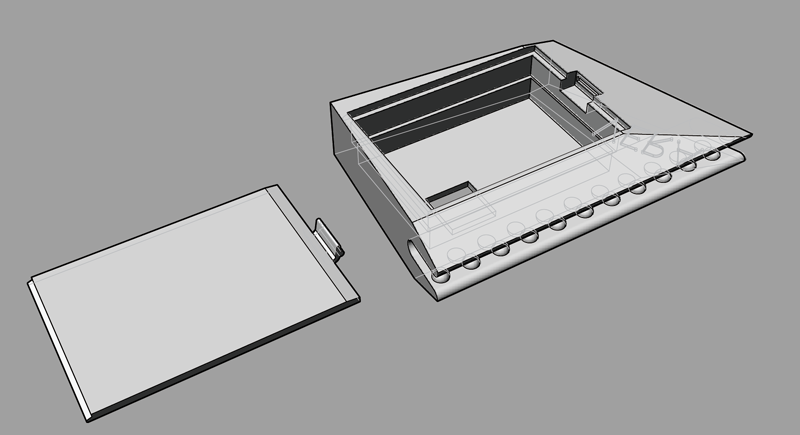
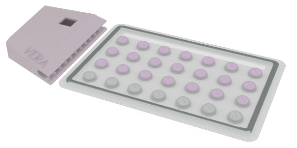
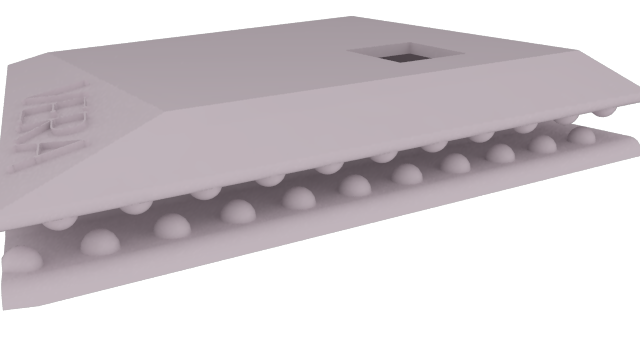
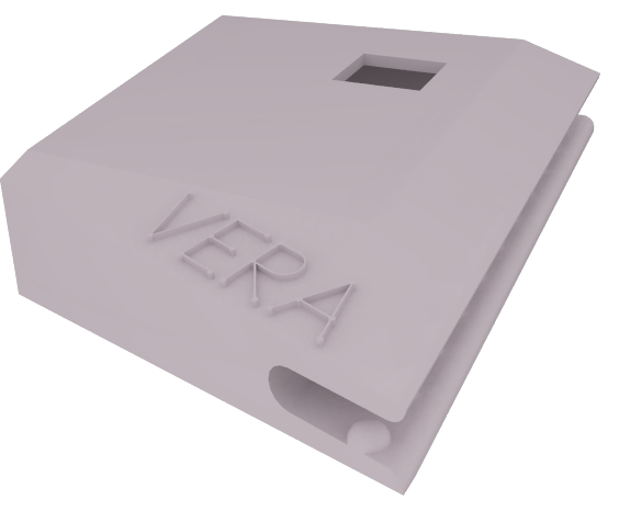
Simultaneous with that was figuring out how the case would look. This is a “test case” mainly because I know that the PCB could be so so so much smaller and narrower, which dramatically affects the design of the overall case, and its unobtrusiveness, which is one of the major important issues here. So I have designed a new case to be 3d printed and sent it out to Shapeways, but… well, I was careful to make sure all the parts were according to their printing parameters for the White, Strong, Flexible material EXCEPT I forgot about checking the lettering of the logo on the top. Two days after I sent it off to print, they sent it back saying that it had to be modified – I modified it and hopefully they’ll still send it to me in time!!!
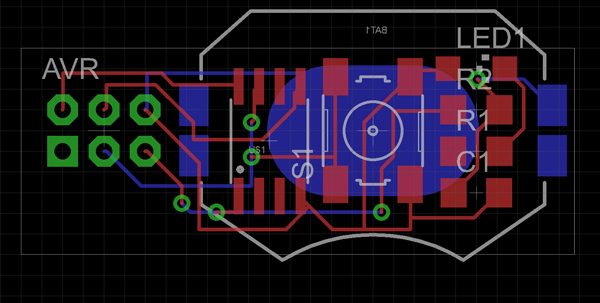
Because I was so annoyed with the size of the case as I’ve designed it, I took another crack at designing the PCB for absolute minimal footprint, and have been able to get it much much narrower… I redesigned a smaller PCB and sent that out, this time to AP Circuits, which seems to have served everyone else in the class much better than Advanced Circuits, which I used for the first board. I’m hoping that I’ll be able to get one of these skinnier boards back in time for the final and stuff and program it, showing that the bulkiness of the case that I’ll have at the final is not something that’s absolutely necessary.
I wish I had started with the PCB design way back in February!! This testing phase has really taught me a lot, not just about Eagle, but also about optimizing all aspects of design for the features you want to have in the product – especially if size matters, as it does here.
